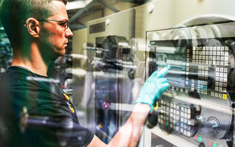
Machining
American Standard Circuits’ PCB CNC milling, machining, and turning services utilize the latest technology. Our PCBA manufacturing services, which include precision machining services and CNC machining services, use machining lathes and milling centers that are on the leading edge of technology and provide unsurpassed speed and machining accuracy. One of the purchasing requirements for our high-speed, high-performance machinery was that the central processing unit (CPU) had to have immediate access to more data and can therefore make many more precise adjustments.
We have carefully chosen high-performance CNC vertical machining centers for their demonstrated accuracy, reliability, and ease of operation. Twenty-four tool stations increase the ability to handle the most complex parts or multi-part set-ups in one machine. Our state-of-the-art PCB CNC milling, machining, and turning centers provide reduced cycle times while ensuring superior position accuracies. These advanced capabilities enable us to deliver quick turn precision machining services for a variety of client needs. With the right combination of power, flexibility, and rigidity, our PCBA manufacturing services offer an ideal solution from prototypes to production runs.
We use precision PCB CNC milling, machining, and turning equipment that provide our clients with high versatility, precision, and productivity. With its 16- tool turret capability, we can machine parts up to 40’ long and 10 diameters.
Your Expert for Machining is Dave Lackey

Dave has been involved with manufacturing PCBs since 1980 and has worked in various shops, most of which had military certifications and utilized higher technology.
Dave has extensive experience building metal-core boards and PCBs requiring thermal management solutions, as well as flex and rigid-flex boards.
Having worked in most departments throughout the years, Dave has developed a strong engineering background and is knowledgeable in most industry technologies. His background enables him to work not only with buyers but design engineers and quality and manufacturing personnel as well. Most questions can be answered on the spot, without having to deal with multiple visits, e-mails, or calls.
American Standard Circuits (ASC) is one of the fastest growing PCB shops in North America. Technology is a key factor contributing to its growth. A few years ago, when Anaya Vardya became CEO of the company, he decided, along with owner Gordhan Patel, the way to grow and thrive in this economy was to drive the company toward not only high-technology, but a wide variety of technologies, from rigid to flex-rigid boards, metal-backed and RF boards, as well as other new technologies using new materials and laminates.
Vice President of Business Development and Technical Sales David Lackey is the company's resident guru when it comes to flex and rigid-flex technology. I recently sat down with him to discuss the technology and its importance to American Standard’s growth and industry growth in general.
Dan Beaulieu: Dave, good talking to you today. Thanks for taking the time. Tell me about your company, especially when it comes to flex and rigid-flex.
Dave Lackey: ASC has been manufacturing PCBs since 1988 and over seven years ago we began building flex and rigid-flex PCBs, a very good direction for us. We are starting to see a lot of interest from our customers--they are trying to get away from wire and incorporate a more reliable connection using flex circuits. We do simple, single-layer flex with LPI or cover-layer up to high-layer-count rigid flex. We keep a fair amount of flex materials in stock and warehoused locally to allow us to respond to quick-turn opportunities in the flex market delivering product in less than five days on many occasions. Our goal is to make it as easy as possible for our customers to design in rigid-flex boards into their products.
Beaulieu: What do you mean by that?
Lackey: Well, in the past, customers had a hard time finding good rigid-flex suppliers. They considered it a hassle to even try to buy flex boards so they designed around them, even though the ultimate product would have benefited by having flex boards. They told us about this and we set about working on being not only the best, but the easiest flex supplier to deal with in North America.
Beaulieu: Dave, can you tell me about your background in the industry? I know you've been around for a number of years and I am always interested in knowing how people got to where they are.
Lackey: I've been doing this for quite a while. I've been manufacturing PCBs since 1980 and have worked in various shops including the captive shop that used to be at Northrop Grumman. A fair amount of my experience has been in shops with military certifications and higher technology. Apart from flex and rigid-flex, I also have a lot of experience building metal-core boards and PCB’s requiring thermal management solutions. Having worked in most departments throughout the years, I've developed a strong engineering background and am knowledgeable in most industry technologies. I spend most of my time in sales now and my background allows me to work not only with buyers, but design engineers and quality and manufacturing personnel as well. This approach tends to satisfy most of the customers' request or questions without having to deal with multiple visits, e-mails, or calls and give customers answers on the spot.
Beaulieu: So your role is more technical sales or maybe applications engineering?
Lackey: Yes, that is correct. Having been the general manager at many PCB facilities, including ASC, I have a strong understanding of not only what our facility needs to be successful, but also what our customers expect from us a supplier of PCBs.
Beaulieu: So ASC is able to handle just about all flex requirements?
Lackey: Pretty much--although we can’t be everything for everybody. American Standard rarely turns away from an opportunity. One of the challenges with flex and rigid-flex is material handling and processing without damaging the product--this is critical. Since we have dealt with fragile and thin-core RF materials for so many years this was a definite advantage. We have developed way to handle the material making sure that it is not damaged during the process. Even though this seems to be a simple thing, it's not...I can assure you. Another concern is registration. Getting good registration on flex boards is very difficult, but because we have invested in all of the necessary equipment and tools, we are in a position to deal with it. In the end, our success is due primarily to our having committed to extensive training on handling and processing of thin cores and we continue to invest in the people and equipment necessary for serving the flex marketplace.
Beaulieu: How has flex technology evolved over the years?
Lackey: I started building flex circuits in 1983. The biggest difference I see between then and now is that there's a lot more rigid-flex now than in the past, which allows designers to utilize BGA and fine-pitch devices on the rigid area yet have the flexibility to use the flex portion to package their devices in confined areas. As we've seen through technology, packaging of electronic devices tends to get smaller and lighter. Flex circuits are a perfect solution to accomplish both. Other changes are the availability of more flex laminate manufacturers and different materials that meet UL criteria, allowing for adhesive-less builds. Additionally, some of the press pad and release materials used for bonding of cover layers and flex multilayers have improved over the years, allowing for improved conformal adhesion to the circuitry and removal of entrapped air along with reduction of adhesive flow onto pads.
Beaulieu: Can you tell us about your customers? What sort of flex applications are out there?
Lackey: We see a wide variety of requirements from our customers, from military and medical devices to simple, single-layer flexes connecting one device to another.
Beaulieu: What advantages does rigid-flex have over normal rigid boards?
Lackey: Packaging and reliability. Rigid-flex boards allow for tighter packaging and the means of connecting multiple devices together without using bulky connectors and multiple PCBs. You ultimately end up with a more reliable product that can be accommodated in tight spaces. Many designers may feel the overall cost of a rigid-flex PCB verses using multiple rigid boards, connectors, and wires is not worth pursuing; however, in many studies we did for our customers depending on the design and use of a rigid-flex replacement the total overall cost and certainly the reliability is usually justifiable.
Beaulieu: What are the major differences between building a flex or rigid-flex board as opposed to building a traditional rigid board?
Lackey: The major differences, other than some varying processes, are registration concerns and handling. Registration is a concern on all PCBs, but given the nature of flex material in itself having proper registration equipment and tools is a major necessity. Handling of the material in itself is a significant challenge. Special material handling carts or trays and training your operators in how to deal with these fragile layers is a must.
Beaulieu: Where do you see the industry going when it comes to flex technology?
Lackey: It's definitely growing. It comes down to reliability of a flex or rigid-flex circuit used as a connector verses wires and the ability to put together a tighter cleaner package for devices. A well laid out design utilizing flex or rigid flex can not only provide the necessary reliability, but also reduces assembly time and rework.
Beaulieu: Why should customers come to you for their flex and rigid-flex boards?
Lackey: In addition our experience and ability to provide a quality flex product we have the ability to do quick-turn builds when necessary. We offer solutions to our customers and their design and packaging engineers who might need assistance with material selections (what can and cannot be done with flex circuits) and we always keep cost in mind. Our goal is to be a total solutions provider not only with our flex offering, but with all of our technologies as well. No customer is too small for American Standard. We have a well-staffed group of talented engineers and a number of outside resources to assist customers early on in the design phase and oftentimes offer alternative options upon receiving a finished design as a method of reducing cost or providing a solution that can provide increased yields.
Beaulieu: Dave, thanks for talking with me today. I appreciate the time you took out of our busy schedule.
Lackey: No problem, Dan. Thank you.Not many companies can do all that American Standard Circuits can and this is why they are succeeding while other companies are struggling. But there is a lesson for all of us here: If we want to succeed in the PCB business we must put the customer first.
Precision CNC machining is inseparable from RF metal-backed PCB manufacturing because the metal carrier, aluminum, copper, or composite, must be machined to exact dimensional specifications before and after bonding to the RF circuit layer. Carrier flatness, pocket depth accuracy, connector landing surfaces, and mounting hole locations all directly affect RF circuit alignment and thermal performance. A non-flat carrier creates airgaps in the bond line that degrade thermal conductivity and affect the dielectric characteristics of the RF circuit above it. In-house CNC machining eliminates third-party subcontract delays, enables tight integration between machining and bonding operations, and supports quick-turn RF metal-backed PCB builds in 5–10 days. American Standard Circuits specializes in advanced HDI PCB fabrication and engineering support.
CNC machining operations on metal carriers for RF PCBs include: precision flatness milling to achieve surface flatness within 0.001 inch for reliable bond quality; pocket machining to recess RF circuit areas for flush or stepped assemblies; mounting hole drilling and tapping for mechanical attachment hardware; through-hole drilling for plated-through connections from the RF circuit layer to the carrier ground plane; edge milling for final outline dimensions; connector cutouts and alignment features; and precision machining of heat spreader fins or cooling channel interfaces on the back face of the carrier. All operations require CNC accuracy appropriate for RF assemblies, where geometric tolerances directly affect electrical performance. American Standard Circuits specializes in advanced HDI PCB fabrication and engineering support.
Metal carrier materials for RF metal-backed PCBs are selected based on thermal conductivity, weight, CTE compatibility with the RF circuit substrate, and machinability. Aluminum (6061-T6, 6062) is the most common choice: lightweight, good thermal conductivity (~160 W/m·K), machinable, and low cost. Copper carriers offer higher thermal conductivity (~385 W/m·K) for high-power density applications but are heavier and more expensive. Aluminum composite materials (AlSiC, Al-SiC MMC) provide intermediate CTE values (8–12 ppm/°C) that better match GaAs or GaN transistor package CTEs, improving thermal cycling reliability. Brass composites are used for specific plating compatibility requirements. Material selection balances thermal, mechanical, and electrical grounding requirements. American Standard Circuits specializes in advanced HDI PCB fabrication and engineering support.
Metal carrier plating provides the electrically conductive surface finish on the carrier that ensures reliable RF grounding, plated-through-hole integrity, and wire-bondable or solderable surfaces. Common carrier plating sequences include: electroless nickel followed by immersion gold (ENIG) for wire-bondable and solderable ground surfaces; hard electrolytic gold over nickel for high-wear connector sliding surfaces; tin or solder plating for sweat solder bonding of PTFE circuits to the carrier; and selective plating of specific regions while masking others. In-house metal carrier plating line capability, separate from the PCB plating line, allows full control of carrier preparation without outsourcing to plating job shops, which would add lead time and quality variability. American Standard Circuits specializes in advanced HDI PCB fabrication and engineering support.
Carrier flatness is critical for RF metal-backed assemblies for two reasons: bond quality and electrical performance. The adhesive or solder bond between the RF PTFE circuit and the metal carrier must be void-free and uniform, any high spots on the carrier create localized pressure during bonding, while low spots create bond-line voids that degrade thermal conductivity and affect the effective dielectric properties of the RF circuit above them. Electrically, variations in bond line thickness alter the effective dielectric height of the substrate, shifting transmission line impedance away from target values. Carrier surfaces are typically specified to less than 0.001 inch (25 micron) total indicated runout (TIR) across the bonding area before lamination. American Standard Circuits specializes in advanced HDI PCB fabrication and engineering support.
RF metal-backed PCB assemblies require multiple sequential processes: PCB fabrication, metal carrier procurement and preparation, carrier plating, precision machining, bonding, and final test. Without in-house machining capability, the carrier machining step requires outsourcing to a precision machine shop, adding scheduling dependencies, additional transportation, and a separate quality control interface. In-house CNC turning and milling centers enable these steps to proceed concurrently or in rapid sequence within the same facility. The result is a 5–10 day quick-turn capability for RF metal-backed assemblies that would otherwise take 3–5 weeks through a multi-vendor supply chain. American Standard Circuits specializes in advanced HDI PCB fabrication and engineering support.
CNC machining for RF PCB metal carriers achieves dimensional tolerances appropriate for high-frequency electronics assembly. Typical achievable tolerances include: ±0.001 inch (±25 microns) on linear dimensions for critical alignment features; ±0.001 inch flatness across the circuit bonding surface; hole position tolerance of ±0.002 inch for mounting and alignment holes; pocket depth tolerance of ±0.001 inch for stepped or recessed circuit areas. For plated-through-hole carrier assemblies, hole diameter tolerance of ±0.002 inch is standard. These tolerances are achievable with modern CNC machining centers using appropriate fixturing and tool selection. Tighter tolerances (±0.0005 inch) are available for specific critical features when required by the assembly design. American Standard Circuits specializes in advanced HDI PCB fabrication and engineering support.
A pre-bond to post-bond assembly conversion is a process that takes a discrete RF PCB (fabricated without a metal carrier) and bonds it to a metal carrier after PCB fabrication is complete, creating what would otherwise be ordered as a post-bonded assembly. The reverse conversion (post-bond to pre-bond) starts with a pre-bonded laminate (PCB substrate already laminated to the carrier from the laminate manufacturer) and fabricates the circuit on the bonded panel. Both conversions offer design flexibility: post-bonding allows yield screening of the PCB before bonding; pre-bonding provides a simpler one-step fabrication process. In-house machining, plating, and bonding capability enables both conversion options within a single facility. American Standard Circuits specializes in advanced HDI PCB fabrication and engineering support.
Precision machining contributes to thermal management in power electronics PCBs by enabling attachment of integral heatsink features directly to metal-core or metal-backed substrates. Machining operations include: fin array machining on the back face of aluminum carriers for natural or forced convection cooling; through-hole drilling for press-fit thermal standoffs; precision milled cavities that position high-power components at specific heights relative to the PCB surface for thermal paste contact optimization; and surface grinding to achieve the flatness required for phase-change material or thermal pad contact. Accurately machined thermal interfaces reduce thermal resistance between component and heatsink by eliminating mechanical contact gaps that act as insulating air layers. American Standard Circuits specializes in advanced HDI PCB fabrication and engineering support.
Edge plating (copper plating on the board edge) and castellations (half-round plated edge contacts) require a combination of routing and plating operations. In the fabrication process, through-holes are drilled in a row along the intended board edge, then copper-plated as part of the standard through-hole plating sequence. The board edge is then routed through the center of the hole row, creating half-circle (castellation) contacts on the board edge. Edge plating of the entire board perimeter requires a slightly different sequence: routing a slot around the perimeter during fabrication, applying copper plating to the slot walls, then performing final routing. CNC routing precision (±0.002 inch) is critical to ensure consistent castellation geometry and edge copper continuity. American Standard Circuits specializes in advanced HDI PCB fabrication and engineering support.