American Standard Circuits is an early adopter of Averatek’s A-SAP process for its ultra high density interconnect (UHDI) products. In this final part of my interview with industry veteran John Johnson, vice president of business development at American Standard Circuits, we use photos, slides, and materials to discuss what he learned from his previous role at Averatek.
Steve Williams: John, let’s talk about the design benefits of UHDI technology.
John Johnson: It’s really amazing what you can do with UDHI technology. There are some things you have to watch out for in a design and because you can do the ultra-fine lines and spaces, a designer has a lot of things in their toolkit. You have via-in-pad plated over microvias, stacked and staggered microvias, and other different structures. But when designing with A-SAP, you first need to focus on using that ultra-fine line and then going to the other design aspects. Maybe use staggered microvias or several levels of staggered microvias and then use a stacked microvia if you really have to. That removes some reliability traps we've had to deal with because we couldn't reach those ultra-fine lines.
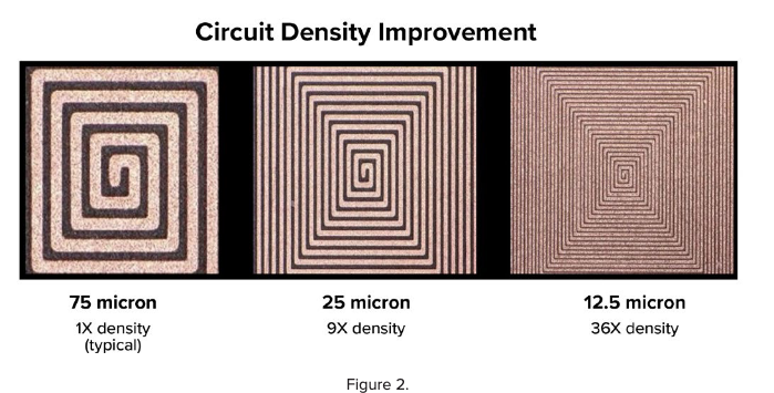
Figure 1 shows what happens when you can achieve ultra-fine features with this technology. Current subtractive technology is around 75 microns, or 3-mil line and space. Some folks can get down to 2 and 2, but it isn’t without some challenge and yield penalty. This technology allows us to get below 25 microns, a present semi-additive capability in
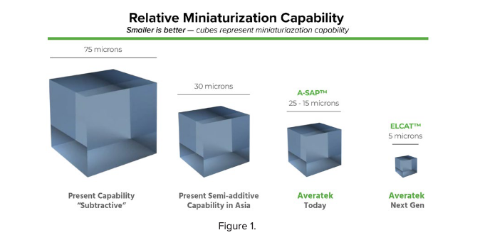
So, 25 microns is 1-mil?
Then sub-1-mil is 15 microns down to 5. It’s almost hard to believe that we can get there. How long until this process comes out?
Is F
I’ve seen some of your samples and you’re right that you have to use some high magnification to even see this definition.
How has the design community accepted and used this, putting out new designs that fabricators like American Standard have to build?
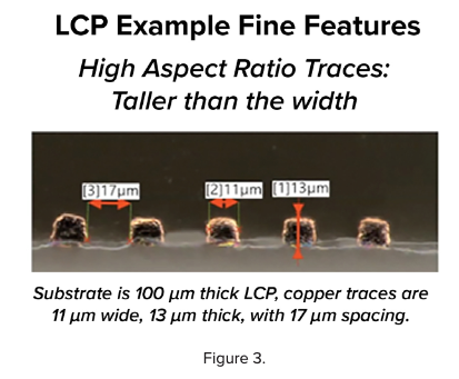
Interesting. John, tell me about Figure 3. What are we looking at?
Earlier you talked about biocompatibility. That’s the beauty of using noble metals that are stable inside the body. If it’s on an LCP or polyimide material, folks are using it in neural probes, glucose monitors, and other types of implantables. Glucose monitors are out there, but whe
We both work with FreedomCAD and we talked about UHDI at the la
I found it incredible that from a design standpoint, you can eliminate virtually 70% of the ball or solder connections. Right, and when you start looking at it, you can get rid of that redistribution layer and solder right down to the chip. It’s pretty amazing.
John, this has been a fantastic discussion. This technology is truly amazing, and it’s something that even 10 years ago nobody could have even dreamed about. You guys are making it happen. It’s very exciting, and that’s the fun part. I enjoy what I’m doing. In this part of my career, the ability to bring this to the point of reality is just fabulous.
I appreciate your time and your expertise on this, and we’ll be talking to you soon. Thanks Steve, I welcome every opportunity to talk about this technology.