American Standard Circuits is an early adopter of Averatek’s A-SAP™ process for its ultra-high density interconnect (UHDI) products. I had the opportunity to sit down with industry veteran John Johnson to discuss this. John previously worked at Averatek and is now vice president of business development at American Standard Circuits where he oversees quality. In the spirit of full disclosure, we will be discussing and sharing photos, slides, and materials with permission from both ASC and Averatek.
Steve Williams: John, American Standard Circuits is a big RF manufacturer. Is there a big application for UHDI in that niche?
John Johnson: Yes, absolutely. From a signal integrity side and getting that straight sidewall, it benefits a lot. But this technology works very well to produce very, very low surface profiles, and that’s an additional benefit. When you look at just building boards with controlled impedance, you can get to a much tighter tolerance. We talk in the industry of typically ±10%, but we can do 5%, so this can get you down to a much tighter tolerance the first time out of the box because you're building right to the design. Your trace will be right there, and since you're plating up a trench—that little trench gets filled up—and that's exactly at the width the designer intended, so it's a lot easier to hit the impedance requirements. Also, this technology has a lot of potential in the medical industry. You can make biocompatible circuit boards because A-SAP does not have any copper or nickel in the construction—which are toxic to the body. You can do traces that are all noble metals like palladium and gold, and that's a big improvement.
Williams: Are you doing anything biocompatible? Johnson: We are. We've built a couple of programs here with more to come. Williams: One of the foundations of the process is liquid metal ink (LMI™). Tell me about that.
Johnson: LMI is a patented Averatek chemistry for putting down a very, very thin coating of palladium on the surface. It’s very dense—basically several levels deep of atoms touching atoms. It’s just a few nanometers thick. That density really helps in getting plating down into all the small crevices and small vias that need to be plated. The liquid metal ink is a non-aqueous base, so that wets very well in all the little nooks and crannies that you'll see in drilled holes. You can metallize these holes much easier than standard plating chemistry...
Now, bear in mind we still do use electrolytes from a variety of manufacturers, so this doesn’t replace electrolytes. It creates that catalyst level that you need to get the plating accomplished, and it works with different me
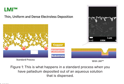
That’s pretty interesting. When you look at the comparison between the LMI and the standard process, it’s striking. Figure 1 illustrates what happens in a standard process when you have palladium deposited out of an aqueous solution that is dispersed. The copper tends to build slower and it’s less dense during the early stages of plating. Over time it will build up a thickness dense enough that w
That’s the key differences. In the SEM image on the right of Figure 1, it shows the electroless deposition, not the palladium, which is so fine that you need a transmission electron microscope to see it. When you look, you’ll see how fine the electroless deposition is, and how it has followed the topography of the copper foil that was there beforehand. That helps to give very good adhesion to that surface.
Is it a special process? Can board shops use their existing processing equipment and tanks, or do they have to put anything special in place?
That’s the interesting thing with this technology; there are very few tanks put in place to get it set up, and very few additional lines to be run. You can use existing lines for flash etching. For example, we use our inner layer clean line—with a mic
Williams: So, it’s not quite a drop-in, but pretty close?
Yes, it’s pretty close. In fact, we have some examples of product we put in for the U.S. Navy, which has been one of the early adopters. Within two weeks we were running panels there that had 25-micron line and space, and the capability with their photolithography to get down further. A few weeks after that, we were running 15-micron, down to 12.5-micron (0.5 mil) line and space. Let me tell you, as someone who has been in this industry a long time, it brought tears to my eyes. It’s just beautiful; that spiral pattern was just awesome. It was zero shorts and zero opens. It’s just a really good process.
In Figure 2, we have a comparison between the A-SAP process and the ultra-thin foil processes that are sometimes called mSAP in Asia. The older mSAP processes started out with a 5-micron foil, an eighth-ounce copper as we would call it in the older days. Now there are foils that are 2-micron and even as thin as a 1.5-micron. So, even with these copper weights, you’re still dealing with a fairly thick base foil that you have to etch. But when you etch something that is only two-tenths of a micron base, it etches very quickly and doesn’t touch the electroplated sidewalls.
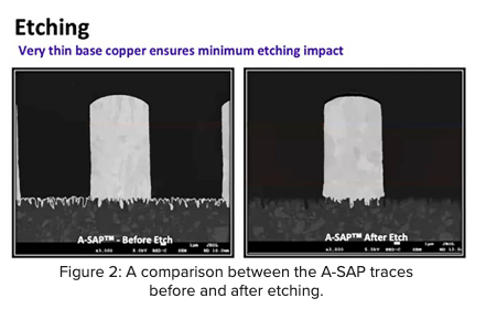
Please talk about your straight edges. This is incredible. It’s really staggering to look at how straight those trace sidewalls are.
On the left, you see the trace that’s been plated. It still shows the electroless down at the base and you can see how thin it is. This trace here is 11 microns wide and it’s about 27 microns high, I believe. When you do the flash etch, you look at that trace and it’s like it hasn’t been touche
That’s just phenomenal. All those rules from way back