Solve Micro Pitched BGA & High Density Circuits Reliably with Ormet® Z-Axis Interconnects
Often people are afraid to use a technology they’re not familiar with, so my hope is to familiarize you with a solution called, “Ormet® Z-Axis Interconnects” that American Standard Circuits is eager to help you utilize. This product has experienced industry acceptance for over a decade and today’s circuit challenges are requiring innovation to meet these challenges. Today’s designs are pushing the barriers on several fronts simultaneously, such as: High-speed circuitry that must meet signal integrity concerns, advanced packaging with µBGA pin pitch requiring (HDI) High-Density Interconnect solutions, along with advanced drilling requirements that can’t be solved with the traditional manufacturing process, such as, back to back buried vias. Ormet® Z-Axis Interconnects meets these challenges head-on. You’ll see it does so reliably with a cost-effective approach.
Ormet® Z-Axis Interconnects are created with a material and process that conductively paste fills a via on any layer, rather than plating the via wall for Z-Axis connectivity. The paste material is an alloy formed from Copper and Tin/Bismuth and the process is called, “(TLPS) Transient Liquid Phase Sintering.” In this article, we are not going to inform you on how the fabricators implement this solution, rather, we wish to explain how you can solve your circuit challenges by utilizing Ormet® Z-Axis Interconnects.
The overview of design challenges we will cover are as follows:
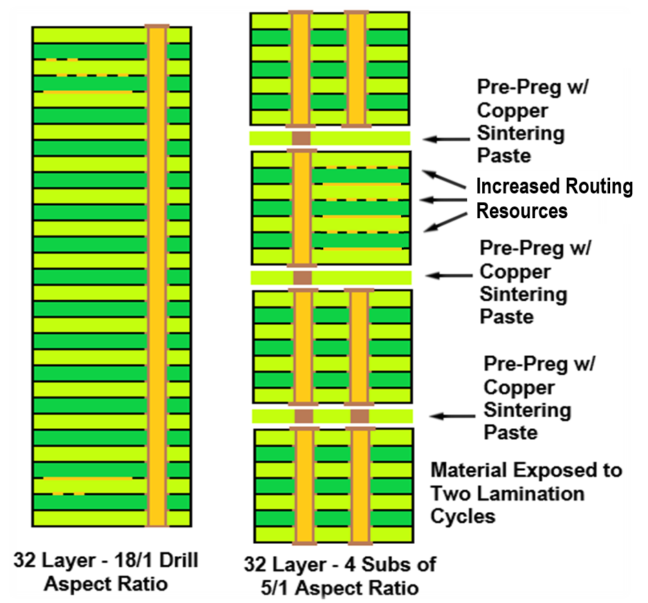
· Reduced Lamination Cycles - Saving time & money
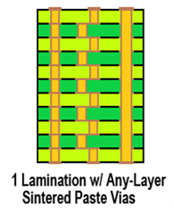
· Any-Layer-Vias HDI = Design freedom
· Eliminate High-Aspect-Vias, used on high layer count boards
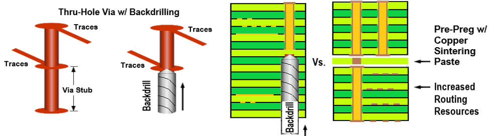
· Eliminate Back-Drilling, no stubs on high-speed signals
· Increase routing resources
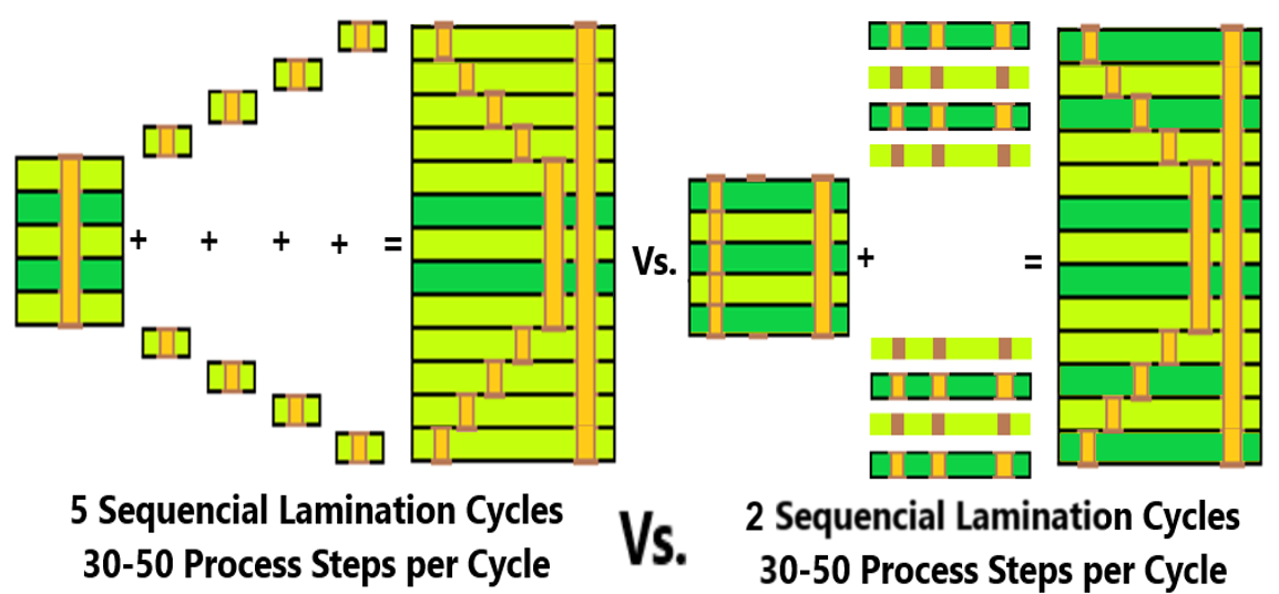
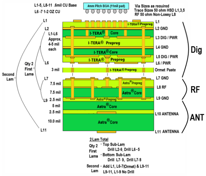
In today’s circuits, µBGAs with a pin-pitch of .65mm or below requires the implementation of HDI. This is no longer a choice but a requirement. The standard method to fabricate these boards is using laser drilled µVias and sequential lamination, whereby a core set of layers typically will have many process steps in a build-up fashion: Adding layers with lamination cycles, drill, etch and plate. Many common HDI builds require 3-5 lamination cycles. Each lamination cycle can consist of approximately 30-50 process steps. Each one of these process steps can add a significant number of days to the fabrication build, with the sum total ranging from 3-5 weeks. All of this adds cost, schedule delays, and threatens long term reliability as the board re-enters a thermal excursion from the lamination heat press multiple times.