
Capabilities
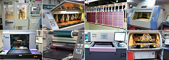
Explore our capabilities
We can manufacture printed circuit boards on virtually any substrate. any size, and any shape. Technology types include, but are not limited to RF/Microwave printed circuit boards, HDI PCB, Blind Via PCB, Micro Via PCB, Cavity PCB, Hybrid PCB, Embedded Passives, Back-drilling PCB, enig PCB, rigid printed circuit boards, metal clad boards, flex PCB, and rigid-flex circuits.
- Layers (1-34)
- Lines and Spaces 3mil line / 3mil space
- Panel Thickness <= 350 mils
- Controlled Impedance +/- 5%
- All types of final finish available
- Blind and Buried Vias
- Heat Sink Technology
- High Performance and Emerging Technology Materials
- Sequential Lamination
- Conductive and Non-Conductive Via Fill
- BGA
- Ultra Fine Pitch
- 25 micron lines and spaces- sub 25 micron coming soon!
- Available on board types- Rigid, Flex and Rigid-Flex.
- Available on all material types.
- Hybrid constructions using Ultra Fine line features on select layers; standard technology on others.
- Microvias to 75 micron with copper filling.
- Tight Impedance tolerances and improved signal integrity.
- Ultra-Fine Line/Space Flex to 25 micron currently- sub 25 micron coming soon!
- Special Flex metallization using only noble metals for biocompatibility (no copper or nickel)
- Single-sided Flex
- Double-sided Flex
- Dual Access
- Stiffeners of Polyimide or FR-4
- Multilayer Flex
- Rigid Flex
- Multilayer up to 22 Layers
- Inplan
- Instack
- Controlled impedance modeling
- Lead free alternative High Tg laminates:
- Example, Isola 370HR, 185HR, Iteq 180A, Ventec VT47, Grace GA170 - Halogen Free Laminates (EMC 528 is an example)
- All Teflon (Rogers, AGC-Taconic/Nelco)
- Standard FR4, FR406, FR408, BT, Cyanate Esters
- Rigid Polyimides and Polyimide Flex
- Megtron/Nelco-13/Isola Itera MT-40
- Ceramic of various types
- OhmegaPly and Ticer Resistor materials
- Faradflex and HK Interra Capacitor materials
- IMS Materials: Aismalibar, (TCLAD now), C-Sem, Laird, Ventec)
- Innerlayer maximum Cu weight: 6oz
- Outerlayer maximum Cu weight: 8oz
- Minimum Cu weight: 1/4 oz
- Minimum core thickness: .002"
- Maximum layer count: 34
- Minimum multilayer thickness: .025"
- Maximum multilayer thickness (non-HASL): .350"
- Maximum multilayer thickness (HASL or LF HASL): .170"
- Blind/buried vias – sequential lamination
- Design and Verification of impedance control
- Minimum conductor width:
Start Cu Foil weight Internal External 0.5 oz. .003" .004" 1.0 oz. .004" .005" 2.0 oz. .005" .006" 3.0+ oz. .006" .007" - Minimum feature spacing:
Start Cu Foil weight Internal External 0.5 oz. .003" .004" 1.0 oz. .005" .006" 2.0 oz. .006" .0075" 3.0+ oz. .007" .009"
- Both IL and OL scanning for circuitry abnormalities
- Minimum feature size capability of 10 microns.
- Scanned to validate customer design data.
- Max. Aspect Ratio: 14 to 1
- Min. hole size tolerance (plated):+ .003" Min hole size tolerance (unplated): +.0015"
- Min. drilled hole size: 6 mil; maximum hole size: 250 mil
- Min. annular plane clearance of drilled hole: .010"
- Min. internal pad size to drill hole size: +.012"
- Min. external pad size to drill hole size: +.010"
- Spray-coated Photo-imageable solder mask
- Screened epoxy solder mask
- Screened UV-curable via plugging
- Peelable mask with stencil
- Min. web thickness: .004
- Min. solder mask clearance : .025
- Dry film solder mask
- Conductive
- Non-Conductive
- Copper Filled Microvias
- Stacked Microvias
- Lead Free HASL - Hot Air Solder Level
- Lead Free Solder
- HASL with Lead
- ENIG PCB - Electroless Nickel / Immersion Gold
- Electroless Palladium
- Electrolytic Hard Gold over Electrolytic Nickel
- Embedded Passives
- Electrolytic Soft gold and Electrolytic Nickel
- Immersion Tin
- Immersion Silver
- OSP - Organic Solder Preservative
- Carbon ink - switch pads
- Scoring - CNC (jump scoring available); Web Routing: available
- Edge milling
- Hard-tool Pierce and /or Blank
- Edge beveling
- Minimum slot width:.020"
- Min. inside radius (milled): .015"
- Min. Distance of Plated Hole to internal Trace or Plane .0075"
- Min. Distance of Non-Plated Hole to internal Trace or Plane: Internal: .0075", External .006"
- Standard finished Minimum Annular Ring is .001", if not specified.
- Min. Pad to Drill Hole Size: Internal .010", External .008"
- Min. Plane Clearance to Drill Hole: .020"
- Min. Drilled Hole Size: .008"
- Dual Access Testing - Universal grid
- Net list Testing (Gerber - extracted/IPC- D-356)
- Fixtureless Testing for Proto/Small Volume
- Impedance Testing (Polar CITS-500) Impedance Tolerance: + /- 5%
- Min. Continuity Test: 10 Ohm
- Max Isolation Test:10 M Ohm
- Voltage: 20 - 1000 VDC
- Fine Pitch Testing:
- Min. SMD Pitch (fixtureless): .012"
- Min. BGA Pitch (fixture): 1 mm (.0394)
- Hipot test: standard 0-2500 VDC, advanced 0-6000VDC
- Flying probe
- RF Telecommunication (500 MHz to 100 GHz); Complex board shapes fabricated using CNC routing, milling; Machining tolerances: ±.005", down to ±.001"; Aluminum-backed PTFE circuit with nickel and gold plating on both copper circuitry and aluminum
- Single and double-sided circuits with thermally conducting electrically insulating bonding film (Thermasil) between circuitry and heat sink base; Copper circuitry with various Cu thicknesses and final finish can be bonded with Al of various types and thickness; For heat management applications: Power supplies, Automotive electronics including LEDs, Computers, Motor controls, and Power semiconductors